1. Introduction: The Hidden Structure Behind the Silicon Revolution
Semiconductor chips power every part of modern life – from smartphones and data centres to electric vehicles and satellites. Yet behind these microscopic miracles lies another kind of engineering marvel: the semiconductor fabrication facility, or also known as simply a fab.
These are not ordinary factories. Each one is a multi billion-dollar structure designed to deliver unimaginable precision, balancing extreme structural stability with flexibility for seismic events.
While the chip may be the star, the structure that enables its creation is an unsung masterpiece of structural engineering. Semiconductor facilities push the boundaries of design codes such as IBC (ASCE, ACI, AISC, etc.), and the Eurocode, combining high-performance materials, vibration control systems, and modular construction techniques. In most cases the client requirements exceed any code defined loading requirements.
This article explores six surprising insights into how these advanced technology facilities are engineered – and why their design challenges are reshaping the future of industrial structural engineering.
2. The Billion-Dollar Case for $15 Billion of Equipment
The first shocking truth: the structure itself represents a fraction of a fab’s total cost.
- Total facility cost: $15–20 billion.
- Structural shell and core: ≈5–10% of cost.
- Process tools and Mechanical, Electrical, and Process (MEP) systems: ≈70–75% of cost.
In other words, the building is a protective shell for an extraordinarily expensive and sensitive ecosystem.
The structural engineering challenge lies not in magnificence but in precision – creating a stable, vibration-isolated environment for multimillion-euro/dollar equipment. This requires:
- Super-flat floors with deflection limits often tighter than L/2000.
- Heavy concrete slabs (up to 1.2 m thick) to reduce floor vibration.
- Vibration isolation pads separating the subfab from the main structure.
All while maintaining loads for elevated slab up to 31.5 kPa (650 psf). Therefore, structural engineers must design not just for strength and stability but for mechanical silence – turning the entire facility into one of the most expensive protective enclosures on Earth.

3. Designing for Absolute Stillness and Violent Shaking
The manufacturing of a modern semiconductor chip is a process of incredible precision. Circuitry line widths are now in the range of 7 to 14 nanometers (nm) – far smaller than a human hair, which averages 80,000 to 100,000 nm wide. At this scale, even the slightest vibration can ruin a batch of chips. Consequently, structural engineers must design for absolute stillness, identifying and isolating every potential vibration source, from internal pumps and fans (which are often placed on springs) to the ambient vibrations from a nearby highway.
This need for a soft, vibration-isolated environment creates a direct conflict with conventional seismic design. To withstand an earthquake, building codes typically require rigid connections that allow a structure to move as a single, durable unit. A “soft” vibration control system would be torn apart, and a rigid seismic system would transmit destructive ground shaking directly to the sensitive tools.
The Vibration Paradox
To achieve this, fabs are designed for absolute stillness, while simultaneously needing to withstand earthquakes. These are conflicting requirements:
- Seismic design (rigid) → the structure must move as one, dissipating energy through ductility.
- Vibration control (soft) → internal floors must be decoupled to isolate sensitive tools.
The Box-in-Box Solution
The solution is ingenious: a “box-in-box” structure.
- The outer box (main structure) handles lateral loads, per Eurocode 8 or ASCE 7.
- The inner box (cleanroom) rests on seismic isolators or inertia pads.
During an earthquake, the outer structure can move independently while the inner cleanroom remains stable. This decoupled system protects process tools and prevents mechanical resonance between structural elements.
In practice, structural engineers perform Finite Element Analysis (FEA) vibration to confirm floor frequencies exceed 15–20 Hz, ensuring no overlap with tool resonance frequencies.

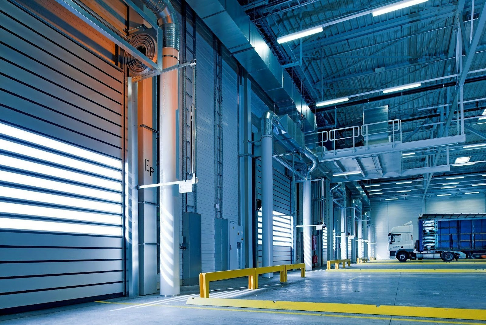
4. The Air That Moves Like a Hurricane (and Must Stay Cleaner Than Surgery)
The term “cleanroom” fails to capture the extreme reality of a semiconductor fab’s production environment. A typical fab cleanroom maintains an ISO Class 4 standard, allowing for only 10 particles of a certain size per cubic meter of air. This is thousands of times cleaner than a hospital operating room.
Laminar Flow Engineering
To achieve this, air is recirculated vertically in laminar flow through HEPA filters and perforated raised floors. Air exchange rates can reach 600 changes per hour – 100 times greater than an office building.
This airflow generates enormous loads on the structure:
- Fan decks and plenum chambers impose concentrated loads of 4-6 kN/m².
- Raised access floors must remain rigid to prevent vibration amplification.
- Suspended ceilings require dense structural grids for MEP coordination.
Structural engineers use steel trusses or composite beam systems to create large, column-free spans while maintaining stiffness.
In addition, the subfab level beneath the cleanroom supports thousands of pumps, chillers, and process tools – each with dynamic vibration profiles that must be isolated from the main slab.

Structural Engineering’s Importance in Semiconductor Fab Design
5. Robots, Pipes, and the Automation-First Layout
While humans work in and around fabs, the internal layout of the cleanroom is not designed for their convenience. Instead, it is dictated entirely by the needs of automation and the efficient delivery of utilities. Many fabs utilize a “spine layout” concept, where an Automated Material Handling System (AMHS) forms a central corridor, like a spine, with all the process bays arranged alongside it. This design minimizes the travel distance for robotic wafer carriers, protecting them from shock and vibration.
The entire facility is often planned using an “inside-out” approach. Rather than starting with property lines and external constraints, designers begin with the optimal layout of the process tools within the cleanroom. The rest of the facility, including the utility buildings, is then designed around this core to minimize the length and complexity of the thousands of pipes and ducts that deliver specialty gases, ultrapure water, and chemicals. For example, wet chemical dispense rooms might be placed on one side of the fab to serve the wet etch area, while specialty gas rooms are placed on another side to serve the deposition area, optimizing the conveyance of each utility.
This automation-first approach directly influences the structural design. As robotic systems evolve from floor-based vehicles to heavier, more complex ceiling-hung networks, the roofs and support structures must be engineered to handle significantly heavier and more dynamic loads.
Inside-Out Planning
Engineers start with the process tool layout and utility requirements – then build the structure around them. This ensures:
- Shorter utility runs and reduced pressure losses.
- Minimal vibration transmission through pipe racks and cable trays.
- Efficient robot paths via the AMHS spine.
Ceiling-Mounted Automation
Modern fabs use ceiling-suspended monorails or robotic conveyors to transport wafers. The roof structure must resist dynamic loads and impact factors from these moving systems.
Typical requirements:
- Additional 2–3 kN/m² live load for suspended systems.
- Localized point loads up to 20 kN from hangers.
- Deflection limits often L/1000 or tighter to maintain alignment.
Therefore, steel design becomes critical – optimizing members for both stiffness and integration with BIM coordination models. The use of Revit and Navisworks ensures that structure, MEP, and architecture align with millimetre precision.
Chapter 16 Structural Design – International Building Code (IBC)
6. Concrete, Steel, and Water: Industrial-Scale Quantities
To truly grasp the scale of these projects, one must move beyond architectural blueprints and look at the sheer volume of raw materials consumed. The construction of a single advanced fab is not merely a project; it is an act of industrial mobilization on par with building the world’s most iconic superstructures. Data from just one Intel factory illustrates this reality:
- Concrete: The project required 600,000 cubic meters of poured concrete. That is twice the amount used to construct the Burj Khalifa, the world’s tallest building.
- Steel: The facility used 35,000 tons of structural steel, which is five times the weight of the Eiffel Tower.
- Water: Fabs are incredibly water-intensive, using millions of gallons daily for cooling equipment and for the multi-step process of cleaning silicon wafers. This immense demand necessitates the construction of large, dedicated water reclamation and storage facilities on-site. These systems not only reduce the impact on the local water supply but are also critical for supporting green building initiatives and ensuring operational continuity.
Structural Material Design
- Concrete is designed to Eurocode 2 or ACI 318 standards with strict shrinkage control to prevent micro-cracking under vibration.
- Steel structures follow Eurocode 3 or AISC 360, using high-strength grades (e.g., S355 or ASTM A913 Gr. 65).
- Composite decks and reinforced mat foundations are analysed for settlement and vibration damping.
How a Semiconductor Factory Works – Newsroom
Sustainability and Reuse
Due to their vast footprint, semiconductor projects also integrate sustainability goals – for example, water reclamation plants and energy recovery systems structurally supported within the same footprint.
Structural engineers must therefore combine strength, serviceability, and sustainability, ensuring compliance with ISO 14001 environmental standards.
7. Managing the Human Risk: Impatience in Fast-Track Projects
For all the technical complexity involved, one of the greatest risks in building a semiconductor fab is entirely human: impatience. The semiconductor market moves at a blistering pace, putting immense pressure on companies to get new facilities online as fast as possible. This often leads to projects being “fast-tracked,” with construction starting even as the fundamental schematic design is still ongoing.
Semiconductor clients often demand “first wafer out” in record time, forcing engineers and contractors to design while building. This fast-track approach can lead to:
- Incomplete load path coordination.
- MEP clashes within structural zones.
- Inefficient sequencing of concrete and steel packages.
Experts in design management recommend that a project of this scale should have a minimum of six to seven months dedicated to design before any construction begins. Rushing the initial planning phase to save a few months on the schedule can introduce design flaws, coordination errors, and inefficiencies. These problems can lead to costly rework and, more importantly, can create issues that will plague the multi-billion dollar facility’s performance and maintenance for its entire 20- to 30-year operational lifespan. For these first-of-their-kind projects, a true partnership model between the owner and the construction contractor is essential to manage the complexity and avoid the long-term consequences of a rushed start. Early investment in BIM coordination, project acceptance criteria definition, and design reviews dramatically reduces rework later.
A Design-Build partnership model, with clear RACI roles between the owner, contractors, specialized vendors, MEP, architectural and structural design teams, ensures quality and safety without compromising speed.
Optimizing Semiconductor Facility Design with BIM: Insights from Intel FAB38 | BIM
Project management in construction : fast-tracking – Perform Effectively
Conclusion: Engineering the Future of the Digital World
Semiconductor facilities represent the pinnacle of structural engineering. They merge the precision of laboratory environments with the scale of heavy industry. Each facility demands the flawless orchestration of:
- Seismic isolation and vibration control.
- Cleanroom airflow engineering.
- Steel and concrete design to Eurocode and IBC standards.
- Advanced BIM coordination across structural, MEP, and process disciplines.
These structures are more than factories – they are monuments of precision, where structure serves science.
As the world races toward smaller transistors and larger fabs, structural engineers will continue pushing design boundaries – building not just for today’s chips but for the digital infrastructure of the next century.
Learn more about industrial structure design at Tine Engineering